
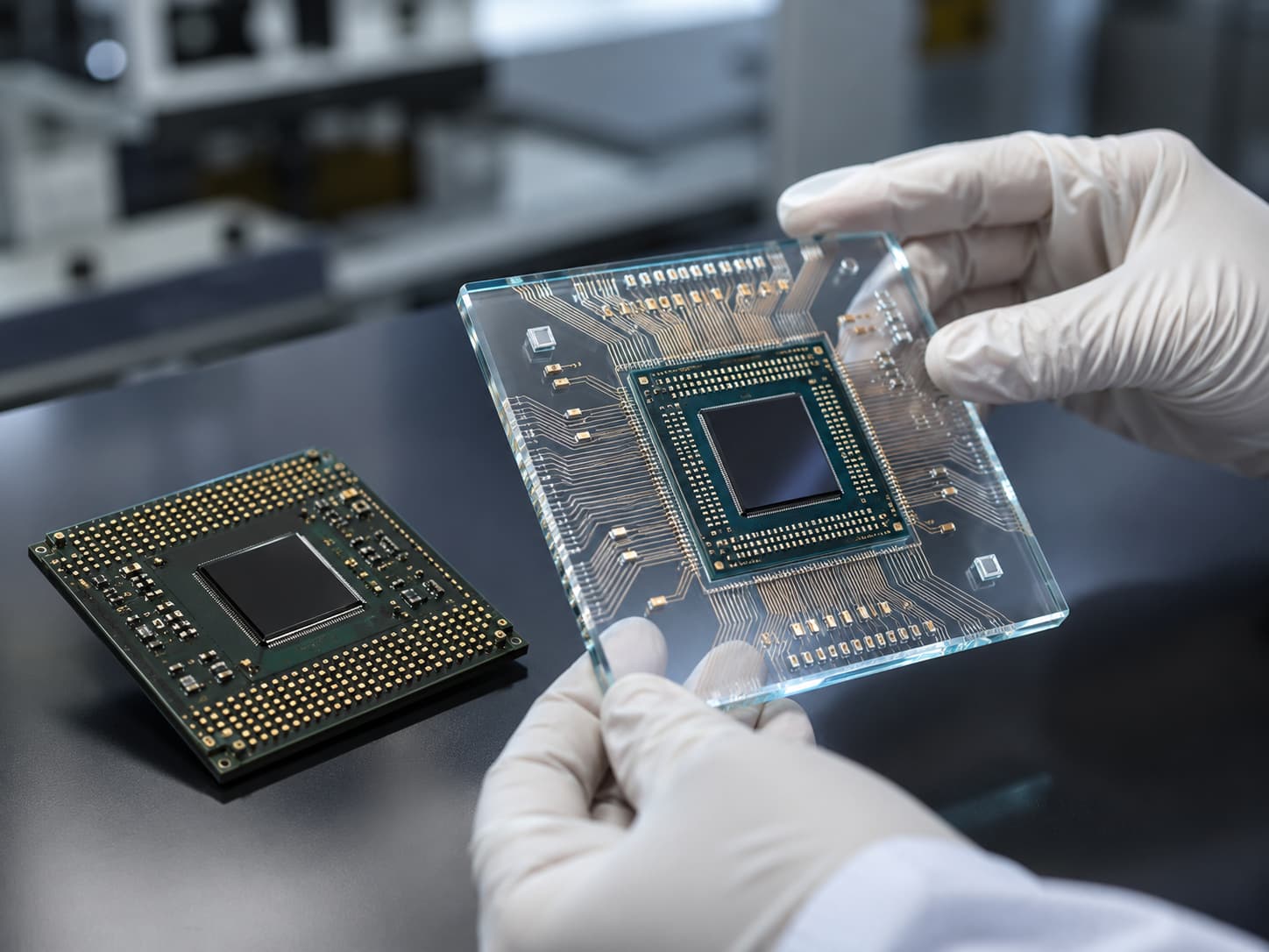
For nearly thirty years, one humble component has quietly sat at the foundation of almost every advanced processor: the packaging substrate, the base layer onto which a chip is mounted and through which it connects to the rest of a device. For all that time, that base has been made of organic materials, essentially sophisticated plastic resins and laminates. It was cheap, it worked, and the industry rarely gave it a second thought. That era is now ending. Under the crushing demands of modern chips, organic substrates have hit a physical wall, and the industry’s biggest players are racing to replace them with an unlikely successor: glass.
The wall that organic substrates hit
The problem is one of heat and scale. Modern processors, especially those built for artificial intelligence and high-performance computing, run hotter, draw more power, and grow physically larger than anything the substrate was originally designed to carry. Organic materials do not cope well with this. Under thermal stress they expand and warp, a failure that engineers have come to call the warpage wall. When the base beneath a chip bends and distorts, the incredibly fine connections between layers can misalign or break, and the whole package becomes unreliable. For decades this was a manageable nuisance. With today’s power densities approaching kilowatt levels on a single package, it has become a hard limit that no amount of clever engineering with plastic can overcome.
This matters because packaging is no longer the boring afterthought it once was. As shrinking individual transistors becomes ever harder and more expensive, much of the recent progress in chips has come from packaging, from the art of stitching multiple pieces of silicon together into one dense, high-performance whole. The substrate is the stage on which all of that assembly happens, and if the stage cannot hold steady, the performance on top of it suffers. The material limit of organic substrates, in other words, had become a limit on the entire industry.
Why glass solves the problem
Glass turns out to be almost ideally suited to fix exactly these weaknesses. It tolerates far higher temperatures than organic resin without deforming. It stays remarkably flat, offering the ultra-low surface distortion that precise manufacturing demands. And it holds its dimensions with the stability needed to keep the tight layer-to-layer connections perfectly aligned even as the package heats and cools. According to figures shared by the technology’s champions, glass can cut pattern distortion by roughly half compared with organic materials.
The practical payoff of these properties is dramatic. Because glass stays flat and stable, engineers can pack the interconnects far more densely, with claims of up to a tenfold increase in interconnect density. They can also build much larger packages, which is essential for the sprawling multi-chip designs that pair processors with stacks of high-bandwidth memory. The mechanical strength of glass allows these oversized packages to be assembled with high yields, meaning fewer are ruined in production. Taken together, these advantages point toward a future of enormous, ultra-dense super-packages that organic substrates simply could never support.
A race among the giants
What makes this a genuine news story rather than a distant laboratory curiosity is that the biggest names in semiconductors are now moving on it in earnest. Intel has been the pioneer, pursuing glass substrates for the better part of a decade and building a fully integrated glass research line in Arizona at a cost exceeding a billion dollars. The company recently demonstrated an early sample combining its advanced packaging with a glass core and, crucially, achieving it without the micro-cracks that had long plagued the material, a milestone that marks a decisive step toward commercial reality.
Samsung has thrown its considerable weight behind the technology as well, pursuing it through its component subsidiary with an explicit focus on chips for artificial intelligence. The Korean giant has gone so far as to form a joint venture with a Japanese chemical partner to secure the specialized core glass material it will need, a sign of just how seriously it takes the transition. They are not alone. A cluster of other players, including SK Absolics, AMD, and others, are pushing into the field, while the largest contract manufacturer in the world is taking a more cautious approach, developing its own glass-based panel-level packaging through a pilot line rather than committing to full production all at once.
A shift that will take years
For all the excitement, it is important to be honest about the timeline. This is not a switch that flips overnight. The first mass-production lines are only now coming online, and even the companies leading the charge expect glass substrates to roll out gradually, proving their yields and winning customer certification with limited capacity before scaling up. Broad adoption across the industry is expected to unfold over a span of years rather than months, and some related applications, such as glass interposers that would replace silicon in connecting processors to memory, are further out still.
There are reasons for the caution. Working with glass at this scale is genuinely difficult. It is brittle, prone to cracking under the stresses of manufacturing, and demands entirely new equipment and processes that the industry has spent years and enormous sums developing. The fact that only a handful of companies can afford the investment tells you how high the barrier to entry is. This is a transition being driven by the deepest-pocketed firms in the business precisely because almost no one else can shoulder the cost.
The force behind the change
Underlying all of this is a single driving force: the explosive growth of artificial intelligence. It is the enormous size, heat, and power appetite of AI processors that finally pushed organic substrates past their breaking point and made the move to glass not just attractive but necessary. The memory shortages and packaging bottlenecks making headlines are all surface ripples of the same underlying pressure, the relentless demand for more computing power straining every physical limit of how chips are built.
Seen in that light, the quiet arrival of glass beneath our processors is one of the more consequential material shifts the semiconductor industry has seen in decades. It is easy to overlook, hidden as it is at the very bottom of the chip, invisible to anyone using the finished device. But it is precisely this unglamorous foundation that will determine how far the next generation of processors can go. The organic era served its purpose for a generation. The glass era is now beginning to take shape, one production line at a time.